Back تصنيع دقيق Arabic Microfabricació Catalan Microfabricación Spanish ریزساخت FA Microfabrication French 微細加工技術 Japanese Microfabricação Portuguese Microfabrication SIMPLE Mikrofabrikation Swedish Mikrofabrikasyon Turkish

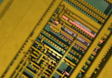
Microfabrication is the process of fabricating miniature structures of micrometre scales and smaller. Historically, the earliest microfabrication processes were used for integrated circuit fabrication, also known as "semiconductor manufacturing" or "semiconductor device fabrication". In the last two decades, microelectromechanical systems (MEMS), microsystems (European usage), micromachines (Japanese terminology) and their subfields have re-used, adapted or extended microfabrication methods. These subfields include microfluidics/lab-on-a-chip, optical MEMS (also called MOEMS), RF MEMS, PowerMEMS, BioMEMS and their extension into nanoscale (for example NEMS, for nano electro mechanical systems). The production of flat-panel displays and solar cells also uses similar techniques.
Miniaturization of various devices presents challenges in many areas of science and engineering: physics, chemistry, materials science, computer science, ultra-precision engineering, fabrication processes, and equipment design. It is also giving rise to various kinds of interdisciplinary research.[1] The major concepts and principles of microfabrication are microlithography, doping, thin films, etching, bonding, and polishing.


- ^ Nitaigour Premchand Mahalik (2006) "Micromanufacturing and Nanotechnology", Springer, ISBN 3-540-25377-7